Showing posts with label Electrical Instrumentation. Show all posts

Sunday 23 July 2017

The History of 555 Timer IC – Story of Invention by Hans Camenzind


The 555 Timer IC is one of the renowned ICs, in the electronic circles. However, its history of invention is not known to many. This article takes you on a journey of 555 timer IC from the time of its creation to the present day time.


What is a 555 timer IC?

A 555 timer IC, is a multipurpose integrated circuit chip, that finds its application in timer, oscillation and pulse generation circuits. It is one of the prominent and popular inventions of the electronic world. A monolithic timing circuit, the 555 timer, is equally reliable and cheap like op-amps working in the same areas. It is capable of producing stabilized square waveform of 50% to 100% duty ratio.


The Birth of 555 Timer IC


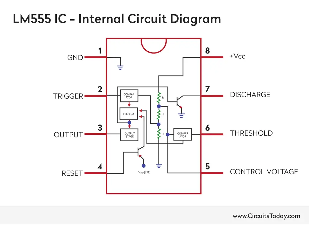
Hans R. Camenzind, designed the first 555 timer IC in 1971, under an American company Signetics Corporation. It is this design work of his, that is most prominent in Hans’s distinguished career in the field of Integrated Circuit technology. In the summer of 1971, first design was reviewed, that used a constant current source and had 9 pins. After the review was passed, Hans thought of a new idea of replacing the constant current source by a direct resistance. This reduced the number of pins from 9 to 8, and enabled the chip to be fit in an 8 pin package instead of a 14 pin package. This new design was passed in the review in October 1971. The IC consists of 25 transistors, 2 diodes and 15 resistors. In order to define the timings, provision to attach R and C externally is provided.


In 1972, Signetics Corp. then released its first 555 timer IC in 8 pin DIP and 8 pin TO5 metal can packages, as SE/NE555 timer and was the only commercially available timer IC at that time. Its low cost and versatility, made it an instant hit in the market. It was later on manufactured by 12 other companies and became the best selling product.

Although, there is a belief that this IC got its name from the three 5k resistors in its internal circuit, Hans R Camenzind revealed in his book, “Designing Analogue Chips”, that it was Signetics manager, Art Fury's, love for the number “555”, that led to the naming of the circuit.

The basic working tutorial of timer 555 IC has been discussed in our article “555timer- A complete guide”.


Applications of 555 Timer IC:

Through the years, electronic hobbyists and engineers have explored various areas where this IC can be used. From temperature measurement to voltage regulators to various multivibrators, this IC has found its prominent place in thousands of applications. The implementation of 555 TIMER IC depends on its operating mode. It is this versatility of 555Timer IC, that makes it useful for many applications.

Basically, a 555 timer IC has three operating modes.
Bi stable mode: The Schmitt trigger
Mono stable mode: One shot mode
Astable mode: Free running mode


555 timer as a multivibrator:

Depending on which type of multivibrator, (astable/monostable or bistable multivibrator) is to be used, the operating mode of 555 timer is selected. For example, if we want to design a monostable multivibrator, we will wire the 555 timer in the monostable mode.

These multivibrators are used in various two state devices such as relaxation oscillators, timers and flip flops.

555 timer IC as a PWM generator:

Using the variable “control” input , a 555 timer IC can be used to create a pulse width modulation (PWM) generator. The duty cycle here, depends on the analogue input voltage.

This operation of 555 timer can also be seen in Switched mode power supply (SMPS)circuit. As these SMPS circuits work on pulse width modulation (PWM) , the 555 timer turns to be the most prominent choice for the designers, as it is cheap and easy to incorporate in a circuit design. Here in these circuits, two timer ICs are used; one operates in astable mode and the other in PWM mode.

Another area where 555timer IC is implemented is in small DC-DC converter circuits. The 555 Timer when operating in astable mode, can produce a continuous stream of pulses of specified frequency. The IC output is fed to the converter to produce desired output voltages. These converter circuits have wide industrial applications.

Other circuits which use 555 timer include that of temperature measurement, moisture measurement waveform generators, various timer circuits, etc.

In recent times, the CMOS version of the IC is most commonly used. Among them, the popular ones are the ICs manufactured by MOTOROLA like MC1455. It can be directly used as a substitute to the original NE555 IC. This IC is pocket-friendly and costs around 0.28 US$.
The bipolar and the CMOS versions of 555 Timer IC

Ever since the first IC was manufactured, over 12 independent companies have fabricated the same. The original design had some design flaws like unbalanced comparators, large operating circuits, and sensitivity to temperature.

Hence, Hans R Camenzind, redesigned the existing IC to diminish the design flaws. The design of this IC was better than its original design. The improved IC was then sold by ZSCTI555 but could not create a buzz like the original 555timer IC did. Hence the original design continued to be a hit in the market.

However, the classic bipolar 555 IC version like NE555 IC, uses bipolar transistors, which dissipate large amount of power and produce high current spikes. Hence, these ICs could not be used in low power applications. This paved a way to the design of a new and version of the same, the CMOS version.

CMOS stands for “complementary metal-oxide semiconductor” and uses a combination of both n-type MOSFET (NMOS) and p-type MOSFET (PMOS), in enhancement mode. All the PMOS transistors have input from either the voltage source or from other PMOS, whereas, all the NMOS transistors have an input connected to ground or to other NMOS transistor. This composition leads to reduction in the power dissipation and lower current spikes.

An example of the CMOS version of 555 timer is LMC555 produced by texas instruments.

The Derivatives of 555 Timer IC:

Now we know what all a single 555 timer IC can do. This means a 555 timer can be used as an oscillator and as a pulse generator in the same circuit. For this purpose, numerous pin compatible derivatives, for both bipolar and CMOS versions of 555 Timer IC were produced by many companies, over the years.

The ICs are available either in round metal can package, or the more commonly seen 8 pin DIP package.


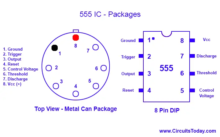
Packages – 555 Timer IC


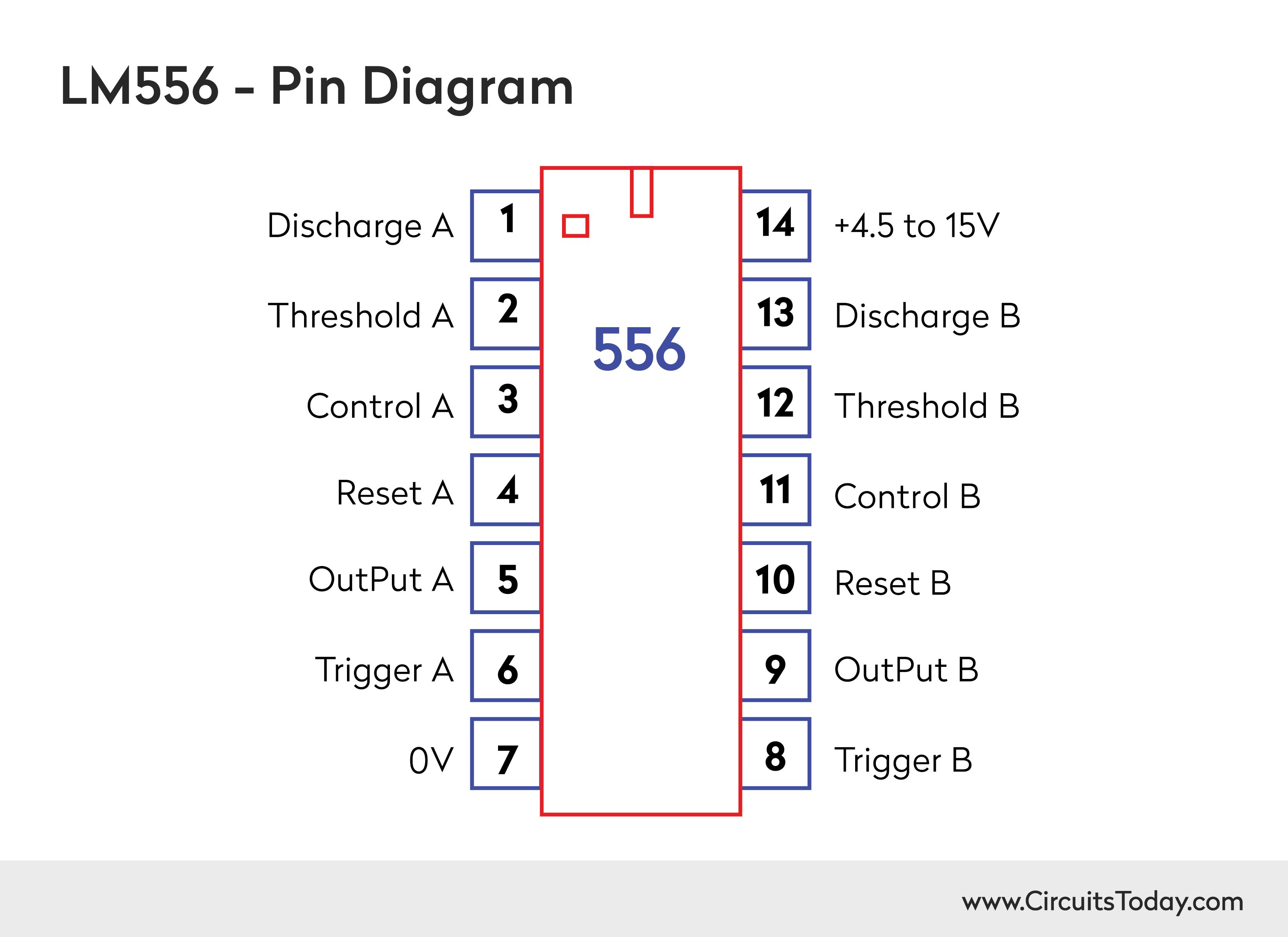
A 14 pin package variation of 555 timer IC, called the 556 IC, was manufactured which had two 555 timer ICs in one chip. Here, the two ICs share a common ground and supply pin. The other 12 pins are allocated to the inputs and outputs of individual 555 timers.

LM556, a dual timer IC manufactured by texas instruments is one such IC. These IC s are ideal for sequential timing application.


Other derivative in 16 bit DIP package, the 558 and 559 had four ICs, in which DIS and THR were connected internally. The 558 IC , is a quad IC and is edge triggered. This eliminates the need of using coupling capacitor for sequential timing applications.
Blogger Widget

Tuesday 5 April 2016

An Introduction about Electrical Relays……

There are two basic classifications of relays:
  • Electromechanical Relays 
  • Solid State Relays 

One main difference between them is electromechanical relays have moving parts, whereas solid state relays have no moving parts.

Electromechanical Relays


Electromechanical relays are switches that typically are used to control high power electrical devices. Electromechanical relays are used in many of today's electrical machines when it is vital to control a circuit, either with a low power signal or when multiple circuits must be controlled by one single signal. 

Advantages of Electromechanical relays include lower cost, no heat sink is required, multiple poles are available, and they can switch AC or DC with equal ease.

Some of the electromechanincal relays are general purpose relays, power relay, contactor and time delay relay.


General Purpose Relay

Well known applications of general purpose relays are:

  • Lighting controls,
  • Time delay controls,
  • Industrial machine controls, 
  • Energy management systems, 
  • Control panels, 
  • Forklifts, 
  • HVAC.

The general-purpose relay is rated by the amount of current its switch contacts can handle. Most versions of the general-purpose relay have one to eight poles and can be single or double throw. 

General Purpose Relays are cost-effective 5.1-15.1 Ampere switching devices used in a wide variety of applications.

These are found in computers, copy machines, and other consumer electronic equipment and appliances.

Power Relay

Power relays are used for many different applications, including:
  • Automotive electronics
  • Audio amplification
  • Telephone systems
  • Home appliances
  • Vending machines
Power relays also contain a spring and an armature and one or many contacts. If the power relay is designed to normally be open (NO), when power is applied, the electromagnet attracts the armature, which is then pulled in the coil’s direction until it reaches a contact, therefore closing the circuit. If the relay is designed to be normally closed (NC), the electromagnetic coil pulls the armature away from the contact, therefore opening the circuit.

Power relay is used for switching a wide variety of currents for applications including everything from lighting control to industrial sensors.

The power relay is capable of handling larger power loads 10-45 amperes or more. They are usually single-pole or double-pole units.

Blogger Widget

Thursday 29 August 2013

3.Electrical Instrumentation lab manual for diploma electrical engineering 3rd sem as per GTU

PRACTICAL 3

AIM: - TEST THE INDUCTANCE BY USING UNIVERSAL IMPEDANCE BRIDGE


OBJECTIVE: - To find the unknown inductance of a coil or inductor using Anderson’s bridge. As a universal impedance bridge.

v APPARATUS:-        
Sl. NO.
NAME
TYPE
RANGE
QTY.
1
Anderson’s bridge circuit


1 no
2.
Head phones


1 no.
3.
Decade inductance box


1 no.
4.
DMM
DIGITAL

1 no.
5.
Patch cards


1set
6
RPS
           
230
1 no
7
Galvanometer


1 no

v CIRCUIT DIAGRAM:
CLICK ON THE LINK


v THEORY :
Anderson’s bridge is a modification of the Maxwell’s inductance capacitance bridge. In this method, the self-inductance is measured in terms of a standard capacitor. This method is applicable for precise measurement of self-inductance over a very wide range of values.
Figure shows the connections and the phasor diagram of the bridge for balanced conditions:
Let L1 = Self-inductance to be measure
R1 = resistance of self-inductor,
r1 = resistance connected in series with self-inductor,
r, R2, R3, R4 = known non-inductive resistances, and
  C = fixed standard capacitor.

At balance, I1 = I3 and I2 = Ic  + I4
Now I1R3 = Lc  x              Ic = I1jωCR3.

Writing the other balance equations
I1 (r1+R1+jωL1) = I2 R2 + Icr and       Ic  = (I2 – Ic) R4.
Substituting the value of Ic in the above equations, we have
I1(r1+R1+jωL1) = I2R2+I1jωC R3r 
Or
I1(r+R1+jωL1-jωCR3r) = I2R2 …(i)
and 
jωCR3 I1     = (I2 – IjωCR3)R4  or  I1(jωCR3r + jωCR3R4 +R3) = I2R4… (ii)

From Eqns. (i) and (ii), we obtain
I1 (r1 + R1 + jωl1 – jωCR3r) = I1  
Equating the real and the imaginary parts : R1 =  
and  L1 = C  [r(R4 + R2) + R2R4]
An examination of balance equations reveals that to obtain easy convergence of balance, alternate adjustments of r1 and should be done as they appear in only one of the two balance equations.

v ADVANTAGES:
1.  In case adjustments are carried out by manipulating control over r1 and r, they become independent of each other.   This is a marked superiority over sliding balance conditions met with low Q coils when measuring axwell’s bridge.   A study of convergence conditions would reveal that it is much easier to obtain balance in the case of Anderson’s bridge than in Maxwell’s bridge for low Q-coils.
2.  A fixed capacitor can be used instead of a variable capacitor as in the case of Maxwell’s bridge.
3. This bridge may be used for accurate determination of capacitance in terms of inductance.
v DISADVANTAGES:
1.   The Anderson’s bridge is more complex than its prototype Maxwell’s bridge.   The Anderson’s bridge has more parts and is more complicated to set up and manipulate.  The balance equations are not simple and in fact are much more tedious.
2.  An additional junction point increases the difficulty of shielding the bridge.
Considering the above complications of the Anderson’s bridge, in all the cases where a variable capacitor is permissible the simpler Maxwell’s bridge is used instead of Anderson’s bridge.


v PROCEDURE :
1.   Connections are made as per the circuit diagram with an audio oscillator and head phones connected to proper terminals of the Anderson’s bridge.
2.   Connect the unknown inductor ‘L’ as shown in the circuit diagram.
3.   Switch on the supply and select a certain value of ‘C’ say 0.01F.
4.   Adjust R1and r1alternately till the head phones give minimum or no sound.
5.   Note down the values of S, M and C at this balanced condition.
6.   Repeat steps (4) and (5) for the same inductance by selecting different value of C.
7.   Repeat the above steps for different values of unknown inductance.
8.   Switch off the supply.

v NOTE : 
1.   The value of ‘C’ is so chosen that there is sufficient adjustment available in the value of M.
2.   When ‘C’ is small, ‘M’ will be large.
3.   The bridge is useful for measuring small values of inductor such as 50, 100, 150 and 200 mH.
Note the value of unknown inductances
1.      10mH
2.      100mH


v OBSERVATION:-

S.NO
C(knowm capacitance)
r1
R1
R2
R3
R4
L1


v CALCULATION :
‘L’ value is calculated by the given formula.     
L1 = C R3/R4 [r1(R4+ R2) + R2R4]
R1 = R2R3/R4-r1

v CONCLUSION:- 

FOR CIRCUIT DIAGRAM ...
PLEASE CLICK ON THE BELOW LINK...


DOWNLOAD link For Practical 3
Blogger Widget

Wednesday 7 August 2013

2.Electrical Instrumentation lab manual for diploma electrical engineering 3rd sem as per GTU

PRACTICAL 2

AIM: - TEST THE LOW RESISTANCE USING KELVIN BRIDGE.


APPARATUS:-
  • Regulated dc supply-1no
  • Standard resistance coil-1no
  • Kelvin’s double bridge kit.
  • Digital multimeter-1no,
  • Patch codes.

CIRCUIT DIAGRAM:-
CLICK ON GIVEN LINK
THEORY:-
               Kelvin’s bridge is a modification of whetstone’s bridge and always used in measurement of low resistance. It uses two sets of ratio arms and the four terminals resistances for the low resistance consider the ckt. As shown in fig. The first set of ratio P
And Q. The second set of ratio arms are p and q is used to connected to galvanometer to a Pt dat an Approx. potential between points m and n to eliminate the effects of connecting Lead of resistance r between the known std. resistance‘s’ and unknown resistance R .The ratio P/Q is made equal to p/q. under balanced condition there is no current flowing Through galvanometer which means voltage drop between a and b, Eab equal to the Voltage drop between a and c, Eamd.
Now
Ead=p/(p+q)
Eab=I[R+S+ ((p+q)r)/(p+q+r)]
Eamd=I[R+ p/p+q [(p+q) r/p+q+r]] 
For zero deflection->
Eac=Ead
[P/P+Q]I[R+S+ {(p+q) r/p+q+r}] =I[R+pr/p+q+r] —______________________(3)
Now, if
P/Q=p/q
Then equation… (3) Becomes
R=P/Q=S-_________ (4)
Equation (4) is the usual working equation. For the Kelvin’s Double Bridge .It indicates
The resistance of connecting lead r. It has no effect on measurement provided that the two Sets of ratio arms have equal ratios. Equation (3) is useful however as it shows the error that is introduced in case the ratios are not exactly equal. It indicates that it is desirable to keep as small as possible in order to minimize the error in case there is a diff. between
The ratio P/Q and p/q.
R=P/QS

OBSERVATION TABLE:-


Sr no.
P                         (Ratio Arm Resistor)

(Ratio Arm Resistor)

S
Standard Resistor

R
Measured Value

R
Actual


PROCEDURE:-
1) The circuit configuration on the panel is studied.
2) Supply is switched on and increased up to 5v.
3) The unknown resistance is connected as shown.
4) The value of P,Q was selected such that a. P/Q=p/q
5) S was adjusted for proper balance and balance value of s was balanced.
6) The value of known resistance was calculated.

PRECAUTIONS:-
1) Check all the connections before turning ON the power supply.
2) Do not exceed the value of 5v.
3) Note the readings accurately.

CONCLUSION:-

FOR CIRCUIT DIAGRAM 
PLEASE CLICK ON THE BELOW LINK.....


DOWNLOAD FILE for practical 2
Blogger Widget